
- PCB Fab
- Etching
- Exposure Machine
- Drilling Machine-Schmoll
- PTH Line
- Solderability Preservative
- Automatic Lamination
- Roll To Roll
- Inner Brown Oxide Line
- CNC Routing Machine
- Laser Direct Imaging
- Immersion Line
- Pre-Treatment
- PCB Assembly
- Automatic Loader
- Screen Printer
- High Speed Chips Mounter
- Multifunction IC Mounter
- Reflow
- Automatic Unloader
- BGA Rework Machine
- Electron Microscope
- Bake Oven
- Oven Temperature Tester
- Components
- Resistance
- Capacitance
- Inductance
- MOS
- MCU/ICS
- DC/DC
- Relays
- Module
- Others
- PCB Design
- AOI
- AOI Inspection
- X-Ray
- X-Ray
- Wave Soldering
- Wave Soldering
- ICT
- ICT
- Anti-Corrosion Paint
- Anti-Corrosion Paint
- Fixture Custom
- Fixture Custom
- LCD Screen Custormization
- LCD Screen Custormization


PCB Capability
PCBAallinone provides 2-64 layered PCBs for fabrication, including Rigid , flex boards ,Rigid-Flex, HDI. Quantities range from prototype to mass production.
Download PCB Capability Detail : 
PCBA Capability
Screen Printer
PCB Size : Min: L48mmxW48mm - Max:L609mm x W508mm
Printing Accuracy :±0.0125mm at 6 sigma, Cpk>2.0
Cycletime Cycle time > 7sec
Wipe the Stencil :Automatic cleaning Stencil system
SlowSnapoffdistance 0.01mm-3.0mm
Front Squeegee(Rear Squeegee) Squeegee pressure can be set
Printspeed Adjustable
MachineStabilitycontrol SPC Data statistics
Operating System :Simple and easy operation interface
Brand: Hitachi; Spec: PXH-1; QTY: 8; Height: 0.3mm~5.0mm PCB size: X:35~335mm Y: 35~255mm
Brand: DEK; QTY: 2
3D Solder Paste;Soldering Testing SPI
Mounter
PCB Size Min: L48mmxW48mm - Max:L510mmxW534mm(Single)
Components Size : Chips 0.6 x 0.3mm(0201) - 18.7 x 18.7mm
ICs 1608~74x74mm(32X180mm) highly:MAX:25.4mm
Placement accuracy:0.09mm (4sigma)/0.05mm(3sigma) cpk≥1.00
Feeder Loading Quantity :248Base Material installation rail,8mm Tape
Brand: FUJI;
Spec: NXT I;QTY: 16
Size: H01: 1608~74mm*74mm 3500cph; Height: 25.4mm
Size: H04: 1608~38mm*38mm 6000cph; Height: 9.5mm
Size: H08: 0402~7.5mm*7.5mm 10000cph; Height: 6.5mm
Size: H12: 0201~5mm*5mm 16000cph; Height: 3mm
Size: H12HS: 0201~5mm*5mm 16000cph; Height: 3mm
(Single: Min50(L)x50(W)~Max534(L)x610(W); Dual: Min50(L)x50(W)~Max534(L)x510(W))
Spec: NXT II; QTY: 16
H12: 0201~5.0
H01: 1608~38.0
H04: 1608~38.0
H08: 0402~7.5
H12: 0201~5.0
H12S: 0201~5.0
H12HS: 0201~5.0
(Single: Min50(L)x50(W)~Max534(L)x610(W); Dual: Min50(L)x50(W)~Max534(L)x510(W))
Spec: NXT V; QTY: 8
Spec: XPF;QTY: 4
Reflow
Solder Paste type: Lead-free solder paste
PCB Size: Min: L48mmxW48mm - Max: L609mm x W508mm
Temperature zone: 8 Temperature zone,2 Cooling zone
Temperature control: Independent Temperature Control
Temperature control precision: ±1℃
PCB transverse temperature deviation: ±1℃
Temperature control range: At room temperature - 350℃
Transmission way: Rail transport
Chip-level placement Opto-Bonder
FINEPLACER femto
Fully automatic sub micron mounter
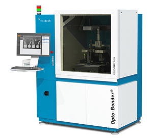
Functional highlights
• Full automatic alignment mode using image recognition
• Full automatic packaging process flow
• 0.5 micron patch accuracy
• wide range of chip sizes
• wide range of chip thickness
• Support 0.05N to 30N patch pressure
• Strong stability
• Component size (min): 0.05 mm x 0.05 mm
• Component thickness: 0.01 mm - 10 mm
• Chip angle fine pitch / resolution: ± 9° / 3.5 μrad
• Worktable Z axis travel / resolution: 10 mm / 0.2 μm
• Worktable Y axis travel / resolution: 150 mm / 0.1 μm
• Worktable X axis travel / resolution: 450 mm / 0.1 μm
• Heating temperature (max): 450 °C
Components:
Electrical testing of electronic components is used to verify that the functionality and characteristics of devices meet correct specifications under a variety of conditions. and electrical testing helps guarantee that devices are functional and within specification. Passive components, such as resistors, capacitors, or diodes, are tested using our digital multimeters and precision LCR meters. Active components, from transistors to microprocessors, require a broader set of stimulus signals and a more advanced data capturing ability. To achieve this, utilizes high-speed high-precision electrical test equipment from leading test equipment vendors. This equipment is designed for both flexibility and extensibility in electrical testing. Current test input and output capabilities include a precision power supply capable of ±20V, ±2A signal generation, a digital signal generator capable of stimulating and capturing digital waveforms at up to 200MHz, and an oscilloscope capable of 14-bit analog waveform capture with a bandwidth of 100MHz. Future upgrade paths include equipment for radio-frequency signal generation and capture. use this equipment to perform electrical testing to military standards, with burn-in, temperature cycling, seal and acceleration testing, and upscreening available to our customers.
Solderability testing, utilizing wetting balance technology, is a measurement of the weight and speed with which the solder meniscus climbs upwards on the component lead dipped in molten solder. When properly administered Wetting Balance measurement is by far the most accurate, quantitative method for measuring, testing and recording solderability. Although the type of Wetting Balance used for through-hole (TH) and surface-mount (SM) components does differ, both are based on the same physical principals.
PCBAallinone Corporation's in-house solderability testing is for both leaded and lead-free components using Multicore Universal Solderability Testers (MUST). The "MUST SYSTEM 3" from "GEN3 Systems" measures the force of solder on a component's electrical connector with a resolution accuracy of >0.01mN. Designed to measure a component's wetting ability or the quality of contact between fluid solder and the component surface, the machine raises a solder module to the component at which point a pulling force is exerted between the solder and the component's electrical connector. The resulting measurement must reach and maintain specific measured parameters for a component to successfully pass solderability. PCBAallinone Corporation performs solderability testing on all open-market sourced product being sold to the Defense & Aerospace industry.
Information Obtained
Force (in mN) needed for proper wetting balance
Lead (+Pb) and Lead-Free (-Pb) solder testing
Graphical report detailing results - (needs to be a link to a solderability report)
Compliances
The MUST SYSTEM 3 Tests to:
IEC 60068-2-69 [-20/-54/-57 Rev]
MIL-STD-883 Method 2022
IPC/EIA J-STD-003A
IPC/EIA/JEDEC J-STD-002B
EIA /JET-7401
Including Edge Dip Test Methods of:
IEC 60068-2-20 and 60068-2-58
IPC/EIA/JEDEC J-STD-002B
IPC/EIA J-STD-003A
To track inventory movement throughout the warehouse, uses the latest warehouse barcode scan system available from Symbol Technologies. This wireless warehouse management tool tracks all product locations, bin storage capacity levels and material FIFO layers. The system allows our warehouse material handlers to sort & locate product based on mfg p/n, internal p/n, lot/dc, fifo and material owner (if consigned product). All material movements are received instantly at the time of scan and all data is redundantly backed up again when reader is back in the charger cradle.
The Acoustic Microscopy method uses a high frequency ultrasound transducer to emit sound waves that are either echoed by or transmitted through a material. The resulting acoustic signature or waveform may be interpreted to determine variations of acoustic impedance within a sample. Differences in acoustic impedance may indicate a change in material densities or separation at an interface. Images can also be generated through a pulse-echo, a means by which the user mechanically scans the transducer across a sample in a raster pattern as it emits and receives an ultrasound signal. An immersion fluid medium is typically used to acoustically couple the samples while analysis is performed.
Acoustic microscopy is a non-destructive screening technique that offers unique insight into the caliber of package and device construction. The advantages of this screening method include the ability to detect void formations, delaminations, cracks and fractures, as well as various other internal defects that may be hidden within inherently susceptible materials and device types. These device types include, but are not limited to:
SOIC
BGA
CSP
Encapsulating Materials
PCB
Molding Compounds
Flex Circuits
All analysis utilizing this method is conducted to IPC/JEDEC J-STD-035 and Acoustic Microscopy for Nonhermetic Encapsulated Electronic Components standards, as well as any additional client requirements.
Compliances
IPC/JEDEC J-STD-035
Information Obtained
Voiding within device
Delamination
Ghost part markings
Resurface material
Instrumentation
Sonoscan D-9000 C-Mode Scanning Acoustic Microscope (C-SAM)
Available to the analysis procedure is the usage of a Through-Scan. Through-Scan transmission mode generates images based on variations in acoustic impedance. This mode is often necessary to verify defects observed during C-Scan mode analysis.
Common Applications
Ceramic Capacitor Defects
Ball Grid Arrays (BGA)
Metal Ball Grid Arrays (MBGA)
Plastic Package Defects
Plastic Encapsulated IC's
Hybrids
Die Attach Defects
Flip Chips
Chip Scale Packages (CSP)
Bonded Wafers
PCBA Lines